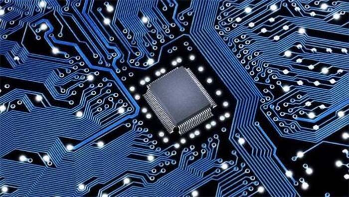
How to design a good PCB board? PCB engineers need to master these PCB design concepts.
PCB design is a technique and an art. Although most of the boards drawn by engineers can be used, the performance varies. How can we design a good board? As an excellent PCB design engineer, you must master the following design concepts.
Signal Integrity (SI)
Signal integrity (SI) refers to the quality of the signal on the transmission path. The transmission path can be an ordinary metal wire, an optical device, or other media.
In the case of short distances and low bit rates, a simple conductor can transmit the signal faithfully.
However, if a long-distance, high-bit-rate signal passes through several different conductors, multiple effects can reduce the credibility of the signal, so that the system or equipment cannot work normally.
As the output switching speed of integrated circuits increases and the density of PCB boards increases, signal integrity has become one of the issues that must be concerned with high-speed digital PCB design.
Factors such as the parameters of the components and the PCB board, the layout of the components on the PCB board, and the wiring of high-speed signals will cause signal integrity problems, resulting in unstable system operation or even no operation at all.
The main issues that need to be considered for signal integrity are ringing, crosstalk, ground bounce, skew, signal loss, and noise in the power supply.
Power integrity (PI)
Power integrity is abbreviated as PI, which is to confirm whether the voltage and current of the source and destination of the power supply meet the requirements. Power integrity is very important in today’s electronic products.
There are several levels of power integrity, chip level, chip package level, circuit board level, and system level.
Among them, the power integrity at the circuit board level must meet the following three requirements.
- Make the voltage ripple of the chip pins smaller than the specifications (for example, the error between the voltage and 1V is less than +/-50mV)
- Control ground bounce (also called synchronous switching noise SSN, synchronous switching output SSO)
- Reduce electromagnetic interference (EMI) and maintain electromagnetic compatibility (EMC).
The power distribution network (PDN) is the largest conductor on the circuit board, so it is also the antenna that is the easiest to transmit and receive noise.
Timing integrity
Timing issues
The extraction of data in the system is usually triggered by the rising or falling edge of the clock signal and is carried out at a certain beat. The data should arrive at the receiving end in time and enter a steady state.
Data timeout delay and data signal distortion will cause data reading errors.
Due to the severe ringing of the signal at the receiving end, some of it enters an unstable state, which will make the data unable to be reliably extracted, causing bit errors.
Basic concepts of time series analysis
Transmission time
Transmission time refers to the propagation delay of the signal on the transmission line and is related to the line length and signal propagation speed.
Flight duration
Flight time refers to the delay between signal transmission from the driving end to the receiving end and reaching a certain level, and is related to the transmission delay and rise time.
Tco
TCO refers to the time difference between the input clock edge trigger of the device and the output signal. This is the sum of all the delays of the signal inside the device.
Establishment time
The setup time refers to the minimum time that the receiver can correctly latch the data and should remain stable before the clock edge comes in. It means the minimum time that the data must be valid before the clock is valid.
Hold time
In order to successfully latch a signal to the receiving end, the device must require the data signal to continue to hold for a period of time after being triggered by the clock edge to ensure that the data is operated correctly. This minimum time is what we call the hold time.
Clock jitter
Clock jitter refers to the random error of the trigger edge of the clock. Clock jitter usually refers to the change of the clock cycle from cycle to cycle. This error is generated internally by the clock generator and has nothing to do with the later wiring.
Clock skew
Clock skew refers to the delay difference between multiple sub-clock signals generated by the same clock.
Electromagnetic compatibility (EMC)
Electromagnetic compatibility (EMC) refers to the ability of a device or system to comply with the requirements in its electromagnetic environment and not produce intolerable electromagnetic disturbance to any device in its environment.
Therefore, EMC includes two requirements: on the one hand, the electromagnetic disturbance generated by the equipment in the normal operation process cannot exceed a certain limit; on the other hand, it refers to the electromagnetic disturbance in the environment. Harassment has a certain degree of immunity, that is, Electromagnetic Susceptibility (EMS).
Testability (DFT)
The testability of product design (Design For Testability. OFT) is also the main content of product manufacturability. From the perspective of production, it is also one of the manufacturability of the design. It refers to the difficulty of testing the product performance when considering the design.
When designing the product, you should consider how to test the performance and processing quality of the product in the simplest way, or the product design should be as easy as possible. Its performance and quality are tested by prescribed methods.
Especially the design of electronic products is essential to product performance testing. The good product design of DFT can simplify the preparation work of inspection and final product inspection in the production process, improve test efficiency, reduce test costs, and easily find product defects and failures, thereby ensuring product quality stability and reliability.
Manufacturability (DFM)
In a broad sense, the manufacturability of a product includes the feasibility of the entire process of product manufacturing, testing, rework, and maintenance. In a narrow sense, it refers to the feasibility of product manufacturing.
Design for PCB manufacturability can be considered from the following two aspects:
- PCB manufacturability (DFM=DesignforManufacture)
- The manufacturability of PCB mounting and assembly. (DFA=DesignforAssembly)
Design for Manufacturability (DFM) is the most effective method to ensure the quality of PCB design. DFM is to consider manufacturability and testability from the time of product development and design so that design and manufacturing are closely linked to achieving the goal of success from design to manufacturing.
DFM has the advantages of shortening the development cycle, reducing costs, and improving product quality. It is a way for a company’s products to succeed.
Reliability
Reliability, we generally say that reliable refers to trustworthiness, reliability is the nature and degree of reliability, which refers to whether the product can be trusted by users when it is used, and its ability to perform its functions and performance normally, accurately, and stably, And how high is the degree.
The reliability of integrated circuits can be divided into reliability design and reliability testing, both of which have accumulated a wealth of experience and technical specifications.
In PCB design work, we need to master these correct design concepts, and then correctly apply them to engineering design and transform them into real products.
You may also be interested in the below articles.
Internal Antenna VS. External Antenna
LTE Vs. 5G: Is 5G Better Than LTE?


