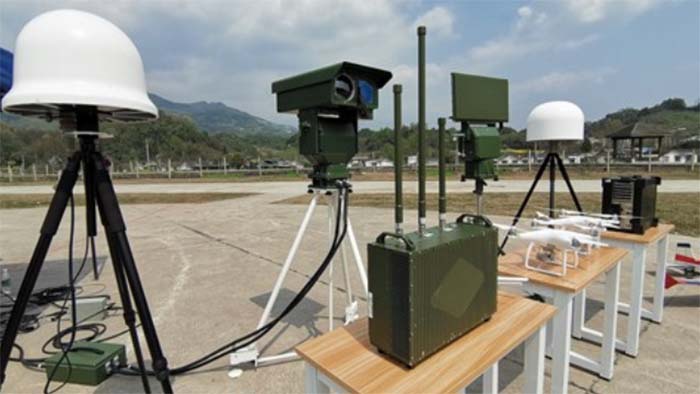
After the read, you will learn about some PCB wiring tips with the Basic Rules And Skills Of PCB Board Wiring.
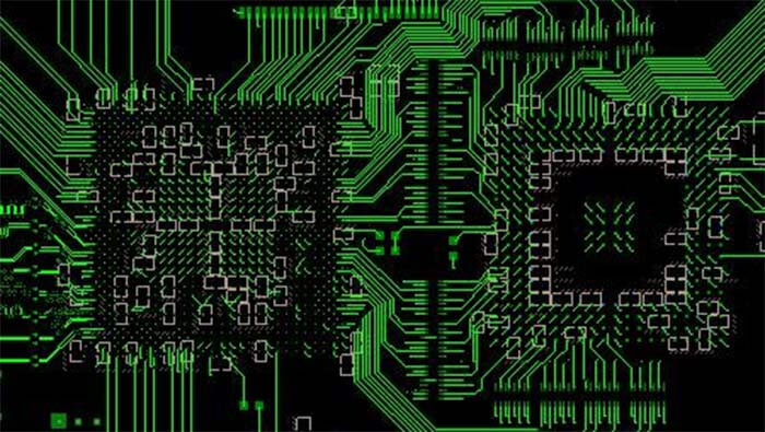
In PCB board design, PCB wiring is an important step to complete product design. In the entire PCB design, the wiring design process is the most limited, the skills are the smallest, and the workload is the largest.
The following are 7 basic rules and techniques for PCB wiring for reference.
1. General rules
1.1 Pre-divided digital, analog, and DAA signal wiring areas on the PCB board.
1.2 Digital and analog components and corresponding wiring should be separated as much as possible and placed in their respective wiring areas.
1.3 The traces of high-speed digital signals should be as short as possible.
1.4 The traces of sensitive analog signals should be as short as possible.
1.5 Reasonable distribution of power and ground.
1.6 DGND, AGND, and ground are separated.
1.7 Use wide cables for power and critical signal traces.
1.8 The digital circuit is placed near the parallel bus/serial DTE interface, and the DAA circuit is placed near the telephone line interface.
2. Component placement
2.1 In the system circuit schematic diagram
a) Divide digital, analog, DAA circuits, and related circuits;
b) Divide digital, analog, and mixed digital/analog components in each circuit;
c) Pay attention to the positioning of the power and signal pins of each IC chip.
2.2 Preliminarily divide the wiring area of the digital, analog, and DAA circuits on the PCB board (general ratio 2/1/1), and keep the digital and analog components and their corresponding wiring as far away as possible and confine them to their respective wiring areas.
Note: When the DAA circuit takes a large proportion, there will be more control/status signal traces crossing its wiring area, which can be adjusted according to local regulations, such as component spacing, high voltage suppression, current limitation, etc.
2.3 After the preliminary division, start placing components from Connector and Jack.
a) Leave the plug-in position around Connector and Jack;
b) Leave space for power and ground wiring around the components;
c) Leave the corresponding plug-in position around the Socket.
2.4 First-place mixed components (such as Modem devices, A/D, D/A conversion chips, etc.)
a) Determine the placement direction of the components and try to make the digital signal and analog signal pins face their respective wiring areas;
b) Place the components at the junction of the digital and analog signal wiring areas.
2.5 Place all analog devices
a) Place analog circuit components, including DAA circuits;
b) The analog devices are close to each other and placed on the side of the PCB containing the TXA1, TXA2, RIN, VC, and VREF signal traces;
c) Avoid placing high-noise components around the TXA1, TXA2, RIN, VC, and VREF signal traces;
d) For serial DTE modules, DTE EIA/TIA-232-E
The receiver/driver of the series interface signal should be as close as possible to the Connector and away from the high-frequency clock signal traces to reduce/avoid the noise suppression devices added on each line, such as chokes and capacitors.
2.6 Place digital components and decoupling capacitors
a) The digital components are placed in a centralized manner to reduce the wiring length;
b) Place a 0.1uF decoupling capacitor between the power supply and ground of the IC, and the connection trace should be as short as possible to reduce EMI;
c) For parallel bus modules, the components are close to the connector is placed on the edge to comply with the application bus interface standard, such as the ISA bus trace length is limited to 2.5in;
d) For serial DTE modules, the interface circuit is close to the Connector;
e) The crystal oscillator circuit is as close as possible to its driving device.
2.7 The ground wires of each area are usually connected at one or more points with 0 Ohm resistors or beads.
3. Signal routing
3.1 In the modem signal wiring, the signal wires that are prone to noise and the signal wires that are susceptible to interference should be kept as far away as possible. If it is unavoidable, use a neutral signal line to isolate.
Modem’s signal pins that are prone to noise, neutral signal pins, and signal pins that are susceptible to interference are shown in the following table:
MODEM signal line
RS-232C serial port signals are divided into three categories: transmission signal, contact signal, and ground wire
(1) Transmission signal: refers to TXD (transmitting data signal line) and RDX (receiving data signal line). The format of the information transmitted via TXD and received by RDX is a transmission unit (byte) composed of a start bit, data bit, parity bit, and stop bit.
(2) Contact signal: refers to the six signals of RTS, CTS, DTR, DSR, DCD, and RI, and their respective functions are as below.
RTS (request to transmit) is a contact signal sent by the PC to the MODEM. A high level indicates that the PC requests to send data to the MODEM
CTS (Clear to Send) is a contact signal sent by MODEM to PC. The high level means that the MODEM responds to the RTS signal sent by the PC and is ready to send data to the remote MODEM.
DTR (Data Terminal Ready) is a communication signal sent by PC to MODEM. The high power screen indicates that the PC is in the ready state, and a communication channel can be established between the local MODEM and the remote MODEM. If it is a low-power screen, the MODEM is forced to terminate the communication.
DSR (Data Device Ready) is a communication signal sent by MODEM to the PC. It points out the working status of the local MODEM. A high level indicates that the MODEM is not in a test call state and can establish a channel with the remote MODEM.
DCD (Transmission Detection) is a status signal sent by MODEM to the PC. The high level indicates that the local DCE has received the carrier signal from the remote MODEM.
RI (ringing indication) is a status signal sent by MODEM to PC. A high level means that the local MODEM has received the ringing signal from the remote MODEM.
(3) The ground wire signal (GND) provides the same potential reference point for the connected PC and MODEM.
The 56K high-speed modem is a dial-up high-speed modem that only started to go on the market in 1997. The reason why its transmission rate can be higher than the limit rate of 33.6Kbps on the traditional telephone line is that it uses a modem technology completely different from 33.6K. Compared with the 33.6 K high-speed Modem, its workpiece principle and usage requirements are also different.
The connection standard between DTE and DCE is CCITTV.10/X.26;
3.2 The digital signal wiring should be placed in the digital signal wiring area as far as possible;
Place the analog signal wiring as far as possible in the analog signal wiring area;
(Isolated traces can be placed in advance to limit, to prevent the traces from being laid out of the wiring area)
Digital signal traces and analog signal traces are perpendicular to reduce cross-coupling.
3.3 Use isolated traces (usually ground) to confine the analog signal traces to the analog signal wiring area.
a) The isolated ground traces in the analog area surround the analog signal wiring area on both sides of the PCB with a line width of 50-100 mils;
b) The isolated ground traces in the digital area surround the digital signal wiring area on both sides of the PCB, with a line width of 50-100 mils, and one side of the PCB should have a width of 200 mils.
3.4 Parallel bus interface signal line width “10mil (usually 12-15mil), such as /HCS, /HRD, /HWT, /RESET.
3.5 Analog signal trace line width> 10mil (usually 12-15mil), such as MICM, MIMV, SPKV, VC, VREF, TXA1, TXA2, RXA, TELIN, TEL OUT.
3.6 All other signal traces should be as wide as possible, line width of “5mil (usually 10mil), and traces between components should be as short as possible (pre-consider when placing components).
3.7 The width of the trace from the bypass capacitor to the corresponding IC is “25mil, and try to avoid using vias.
3.8 Signal lines passing through different areas (such as typical low-speed control/status signals) should pass through isolated ground wires at one point (preferred) or two points.
If the trace is located on only one side, the isolated ground trace can be routed to the other side of the PCB to skip the signal trace and keep it continuous.
3.9 Avoid 90-degree bends for high-frequency signal routing and use smooth arcs or 45-degree angles.
3.10 High-frequency signal wiring should reduce the use of connections.
3.11 Keep all signal wires away from the crystal oscillator circuit.
3.12 For high-frequency signal wiring, single continuous wiring should be used to avoid the situation where several sections of wiring extend from one point.
3.13 In the DAA circuit, leave a space of at least 60 miles around the perforation (all layers).
3.14 Clear the ground loop to prevent unexpected current feedback from affecting the power supply.
4. Power
4.1 Determine the power connection relationship.
4.2 In the digital signal wiring area, use a 10uF electrolytic capacitor or a tantalum capacitor in parallel with a 0.1uF ceramic capacitor and then connect it between the power supply and the ground. Place one place at the power inlet end and the farthest end of the PCB board to prevent noise interference caused by power spikes.
4.3 For double-sided boards, at the same level of the electrical circuit, use power traces with a line width of 200 mils on both sides to surround the circuit. (On the other side, do the same with the digital ground)
4.4 Generally, route the power supply and then route the signal.
5. Ground
5.1 In the double-sided board, the unused areas around and below the digital and analog components (except DAA) are filled with digital ground or analog ground. The same ground areas on each level are connected together, and the same ground areas on different levels are connected by multiple vias. :
The Modem DGND pin is connected to the digital ground area, the AGND pin is connected to the analog ground area; the digital ground area and the analog ground area are separated by a straight gap.
5.2 In a four-layer board, use digital and analog ground areas to cover digital and analog components (except DAA); Modem DGND pin is connected to the digital ground area, AGND pin is connected to the analog ground area; digital ground area and analog ground area are used A straight gap separates them.
5.3 If an EMI filter is required in the design, a certain space should be reserved at the end of the interface socket. Most EMI devices (Bead/capacitor) can be placed in this area; the unused area is filled with land, and if there is a shielded enclosure, it must be connected to it.
5.4 The power supply of each functional module shall be separated. Functional modules can be divided into parallel bus interface, display, digital circuit (SRAM, EPROM, Modem) and DAA, etc. The power/ground of each functional module can only be connected at the source point of the power/ground.
5.5 For serial DTE modules, use decoupling capacitors to reduce power coupling, and the same can be done for telephone lines.
5.6 The ground wire is connected at one point, if possible, use Bead; if necessary to suppress EMI, allow the ground wire to be connected elsewhere.
5.7 All ground wires should be as wide as possible, 25-50mil.
5.8 All capacitor traces between IC power and ground should be as short as possible and do not use vias.
6. Crystal oscillator circuit
6.1 All traces connected to the input/output terminals of the crystal oscillator (such as XTLI, and XTLO) should be as short as possible to reduce noise interference and the influence of distributed capacitance on the Crystal. The XTLO trace should be as short as possible, and the turning angle should not be less than 45 degrees. (Because XTLO is connected to a driver with fast rise time and high current)
6.2 There is no ground layer in the double-sided board. The ground wire of the crystal capacitor should be connected to the DGND pin closest to the crystal on the device with as wide a short wire as possible, and vias should be minimized.
6.3 If possible, ground the crystal housing.
6.4 Connect a 100 Ohm resistor between the XTLO pin and the crystal/capacitor node.
6.5 The ground of the crystal capacitor is directly connected to the GND pin of the Modem. Do not use the ground area or ground wire to connect the capacitor to the GND pin of the Modem.
7. Independent Modem design using EIA/TIA-232 interface
7.1 Use a metal casing. If you need to use a plastic case, you should stick metal foil or spray conductive material inside to reduce EMI.
7.2 Place chokes of the same mode on each power line.
7.3 Place the components together and close to the Connector of the EIA/TIA-232 interface.
7.4 All EIA/TIA-232 devices are individually connected to power/ground from the power source point. The source of the power/ground should be the power input terminal on the board or the output terminal of the voltage regulator chip.
7.5 Connect the signal ground of the EIA/TIA-232 cable to the digital ground.
For the analog signal, some detailed explanations are given:
The design of analog circuits is the most troublesome but also the most fatal part of the design for engineers. Although the current development of digital circuits and large-scale integrated circuits is very rapid, the design of analog circuits is still inevitable, and sometimes digital circuits cannot replace them. , Such as the design of an RF radio frequency circuit!
Here is a summary of the issues that should be paid attention to in analog circuit design. Some are purely empirical. I hope you can add more and criticize and correct me!
(1) In order to obtain a feedback circuit with good stability, it is usually required to use a small resistor or choke outside the feedback loop to provide a buffer for the capacitive load.
(2) The integral feedback circuit usually requires a small resistor (about 560 ohms) in series with each integral capacitor larger than 10pF.
(3) Do not use active circuits to filter or control the RF bandwidth of EMC outside the feedback loop, but only use passive components (preferably RC circuits). The integral feedback method is only effective at frequencies where the open-loop gain of the op-amp is greater than the closed-loop gain. At higher frequencies, the integrator circuit cannot control the frequency response.
(4) In order to obtain a stable linear circuit, all connections must be protected by passive filters or other suppression methods (such as photoelectric isolation).
(5) Use EMC filters, and all IC-related filters should be connected to the local 0V reference plane.
(6) Input and output filters should be placed at the connection of the external cable, and any wire connection inside the unshielded system needs to be filtered because of the antenna effect. In addition, filtering is also required at the wire connections inside the shielding system of the converter with digital signal processing or switch mode.
(7) The power and ground reference pins of analog ICs require high-quality RF decoupling, which is the same as digital ICs. But analog ICs usually require low-frequency power supply decoupling, because the power supply noise rejection ratio (PSRR) of analog components increases very little after being higher than 1KHz. RC or LC filtering should be used on the analog power traces of each op-amp, comparator, and data converter. The corner frequency of the power filter should compensate for the PSRR corner frequency and slope of the device to obtain the desired PSRR within the entire operating frequency range. 2 p% U- S; y3 a8 f
(8) For high-speed analog signals, according to their connection length and the highest frequency of communication, transmission line technology is necessary. Even if it is a low-frequency signal, the use of transmission line technology can improve its anti-interference performance, but a transmission line that is not properly matched will produce an antenna effect.
(9) Avoid using high-impedance input or output, they are very sensitive to the electric field.
(10) Since most of the radiation is generated by common-mode voltage and current, and because most environmental electromagnetic interference is caused by common-mode problems, balanced transmission and reception (differential mode) technology is used in analog circuits It will have a good EMC effect and can reduce crosstalk. The balanced circuit (differential circuit) drive will not use the 0V reference system as the return current loop, so a large current loop can be avoided, thereby reducing RF radiation.
(11) The comparator must have hysteresis (positive feedback) to prevent erroneous output conversion due to noise and interference, and to prevent oscillation at the disconnection point. Do not use a comparator that is faster than required (keep dV/dt within the required range, as low as possible).
(12) Some analog ICs themselves are particularly sensitive to radiofrequency fields, so it is often necessary to use a small metal shielding box mounted on the PCB and connected to the ground plane of the PCB to shield such analog components. Note, to ensure its heat dissipation conditions.
You may also be interested in the below articles.
Internal Antenna VS. External Antenna
LTE Vs. 5G: Is 5G Better Than LTE?