After the read of the article of Secrets of RF Circuit Design, you will learn about the Secrets of RF Circuit Design.
Successful RF design must pay careful attention to every step and every detail of the entire design process, which means thorough and careful planning must be done at the beginning of the design phase, and a thorough and continuous evaluation of the progress of each design step.
Now, let's talk about the secrets of RF circuit design.
In recent years, due to the demand and growth of Bluetooth devices, wireless local area network (WLAN) devices, and cell phones, prompting the industry to pay more and more attention to RF circuit design skills. From the past to the present, RF circuit board design as electromagnetic interference (EMI) issues, has been a difficult part of the engineer’s control, or even a nightmare. If you want to design success, must be carefully planned in advance and attention to detail in order to be effective.
RF circuit board design because there is still a lot of uncertainty in the theory, so it is often described as a black art. But this is only a biased view to cover the whole, RF circuit board design or there are many who can follow the rules. The really practical trick is how to compromise these laws when they cannot be implemented due to various restrictions.
Important RF design topics include impedance and impedance matching, insulation materials and laminates, wavelength and harmonics, etc.
RF Circuit Layout Guide is an extremely critical process in the development of WiFi products. Many times, we may have been well designed in principle, but in the actual production of the board, after the parts were found very unsatisfactory.
These are the reasons for the wiring (Layout) is not done well. This article will take a wireless network card wiring example and a little of my work experience to explain the RF circuit in the wiring should pay attention to some of the issues.
Circuit Board Stack Up (PCB Stack Up)
Before wiring, we must first determine the stack-up of the circuit board, just like building a house to have the walls of the house first. The determination of the board stack up with the complexity of the circuit design, electromagnetic compatibility considerations, and many other factors. The following diagram shows the common stacking methods for four-layer, six-layer, and eight-layer boards.
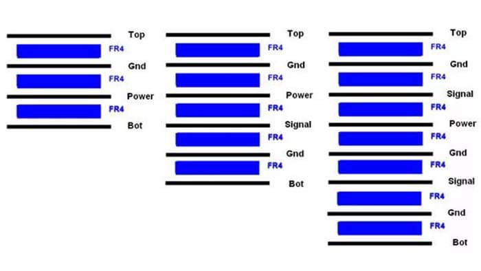
In the PCB stack of wireless cards, there is basically no single panel, this article will not discuss the case of a single panel.
A two-layer board design should be noted in the issue.
In the four-layer board design, we will generally use the second layer as a complete ground plane, also the important signal lines go on the top layer (including RF alignment, of course), in order to facilitate good control of impedance. In a six or more layer board design, we still use the second layer as the complete ground plane, and then put the most important signal lines on the top layer.
You can use Polar to calculate single-ended impedance and impedance, etc. Some Layout software has its own integrated impedance calculator, such as Allegro.
Impedance Control
After we do the schematic design and simulation, one of the things worth noting in Layout is impedance control. We should try to ensure that the characteristics of the alignment are 50 ohms, which is mainly related to the line width, in this example, is two and a half layers, in Polar using Surface Coplanar Line model for impedance calculation, we can get a set of ideal values:
Height(H) = 39.6mil, Track(W) = 30mil, Track(W1)=30mil, Thickness=1OZ=1.4mil, Separation(S)=7mil, Dielectric(Er)=4.2, corresponding to a characteristic impedance of 52.14 ohms, which meets the requirements.
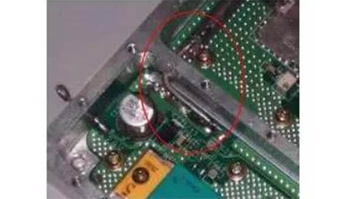
The highlighted line in the figure below is such an RF alignment.
RF component placement
We should make the length of the alignment as short as possible, and the more compact the components are placed, the better (except for special requirements). Try to ensure the placement of components as much as possible, which is very beneficial to the wiring (do not make the wiring go around). The following figure is the placement of an RF power amplifier around the device, we see that the distance between components is very small.
RF alignment attention points
As mentioned before, the length of the RF alignment should be as short as possible, and the line width should be set in strict accordance with the calculated value. In the alignment is particularly important to note is that the RF alignment should not have any sharp fold, in the turn of the line, it is best to use the arc to achieve, as following picture shows.
Secondly, in the multilayer board alignment, there may be important RF lines to produce the inevitable cross, then we have to use the over-hole. In this way, there will be part of the RF signal line to the bottom or even the middle layer, but no matter which layer, RF alignment will certainly have a reference plane, which is a noteworthy issue is not to cross the layer, or do not make the ground plane is not continuous.
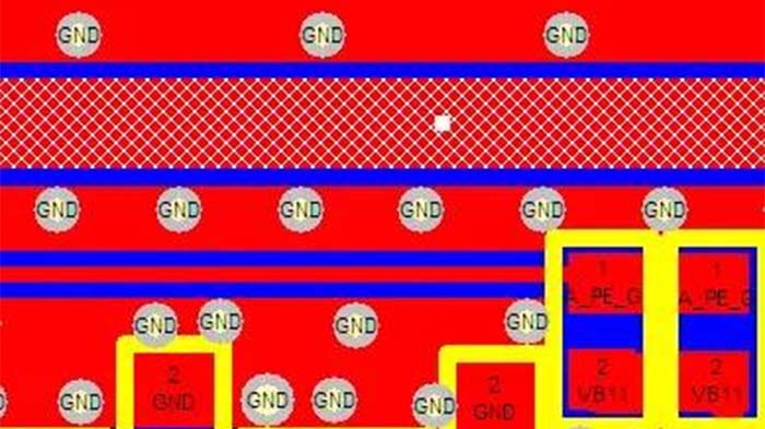
The placement of the hole
The placement of the over-hole is really a complex matter, this article only discusses the kind of grounding over-hole.
Firstly, the RF alignment of the ground line is better through the hole to the ground plane of the bottom or middle layer, then any interference signal or radiation has the shortest path to the ground. The distance between the hole and the RF signal line can not be too close, otherwise, it will seriously affect the quality of the RF signal.
Secondly, in the larger area of the ground plane, we usually place a lot of holes for connecting different layers of ground. With the wiring of RF circuits, it is best to get a diamond shape so that you can maximize the suppression of a variety of interference.
RF circuit power supply design
(1) power line is an important way of EMI out of the circuit.
Through the power line, external interference can be transmitted into the internal circuit, affecting the RF circuit indicators. In order to reduce electromagnetic radiation and coupling, the DC-DC module is required to minimize the primary side, secondary side, and load side loop area. The power supply circuit, no matter how complex the form, is a high-current loop that should be as small as possible. Power and ground lines should always be placed very close together.
(2) If a switching power supply is used in the circuit, the layout of the peripheral devices of the switching power supply should conform to the principle of the shortest path of each power return. Filter capacitors should be placed close to the relevant pins of the switching power supply. Use common-mode inductors close to the switching power supply module.
(3) Long-distance power cables on a single board cannot be approached at the same time or pass near the output and input terminals of the cascade amplifier (gain greater than 45dB). Avoid the power line from becoming an RF signal transmission path, which may cause self-excitation or reduce the sector isolation. High-frequency filter capacitors need to be added to both ends of long-distance power lines, and even high-frequency filter capacitors are added in the middle.
(4) RF PCB power supply entry at the combination of three filter capacitors in parallel, using the respective advantages of the three capacitors to filter out low, medium, and high frequencies on the power line. For example 10uf, 0.1uf, 100pf. and in order from largest to smallest near the input pin of the power supply.
(5) To feed the small-signal cascaded amplifier with the same power supply, you should start from the final stage, and then supply power to the previous stage in turn so that the EMI generated by the final circuit has less impact on the previous stage. And each level of the power filter has at least two capacitors: 0.1uf, 100pf. When the signal frequency is higher than 1GHz, a 10pf filter capacitor should be added.
(6) Commonly used in low-power electronic filters, the filter capacitor should be close to the transistor pin, and the high-frequency filter capacitor should be closer to the pin. The triode chooses the lower cut-off frequency.
If the triode in the electronic filter is a high-frequency tube, it works in the amplifying area, and the layout of the peripheral components is unreasonable, and it is easy to produce a high-frequency oscillation at the output end of the power supply.
The linear voltage regulator module may also have the same problem. The reason is that there is a feedback loop in the chip and the internal triode is working in the amplifying area. In the layout, the high-frequency filter capacitor is required to be close to the pin to reduce the distributed inductance and destroy the oscillation condition.
(7) PCB POWER part of the copper foil size in line with its maximum current flow, and consider the margin (general reference for 1A/mm line width).
(8) The input and output of the power supply line should not be crossed.
(9) Pay attention to power decoupling, and filtering, to prevent interference between different units through the power lines, power supply wiring should be isolated from each other. Power lines are isolated from other strong interference lines (such as CLK) with ground lines.
(10) small-signal amplifier power wiring needs ground copper skin and ground over-hole isolation, to avoid other EMI interference fleeing into, and then deteriorating the signal quality of this level.
(11) different power supply layers in the space to avoid overlap. Mainly to reduce interference between different power supplies, especially some voltage differences between the power supply, the overlap of the power plane must try to avoid the problem, difficult to avoid when you can consider the interval ground layer.
(12) PCB board layer allocation is convenient to simplify subsequent wiring processing. For a four-layer PCB board (a commonly used circuit board in WLAN), in most applications, the top layer of the circuit board is used to place components and RF leads, and the second layer is used as the system ground, The power part is placed on the third layer, and any signal lines can be distributed on the fourth layer.
The second layer adopts a continuous ground plane layout, which is very necessary to establish an RF signal path with controlled impedance. It is also convenient to obtain the shortest possible ground loop and provides a high degree of electrical isolation for the first and third layers so that the two couplings between the layers are minimal.
Other board layer definition methods can also be used (especially when the circuit boards have different numbers of layers), but the above structure is a proven successful example.
(13) A large area of the power layer can make Vcc wiring easy, but this structure is often a fuse that causes system performance degradation. Connecting all the power leads together on a larger plane will inevitably prevent the pin between the pins. Noise transmission.
Conversely, if a star topology is used, the coupling between different power supply pins will be reduced.
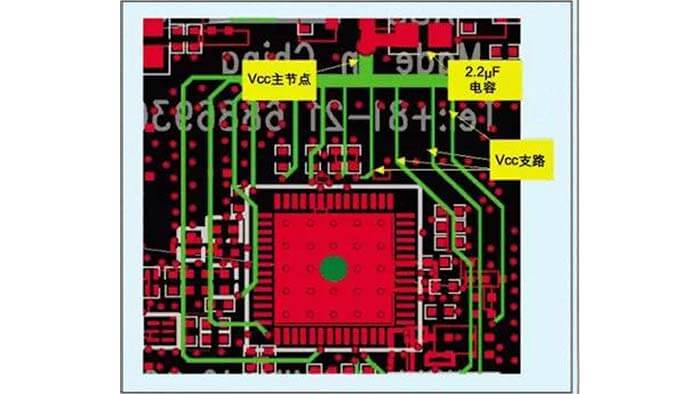
The figure above shows the Vcc wiring scheme for star connection. This figure is taken from the evaluation board of the MAX2826 IEEE 802.11a/g transceiver.
In the figure, a main Vcc node is established, from which power lines of different branches are drawn to supply power to the power pins of the RF IC.
Each power supply pin uses an independent lead to provide spatial isolation between the pins, which is beneficial to reduce the coupling between them. In addition, each lead also has a certain parasitic inductance, which helps filter high-frequency noise on the power line.
When using the star topology Vcc lead, it is also necessary to take appropriate power decoupling, and the decoupling capacitor has a certain parasitic inductance. In fact, the capacitor is equivalent to a series RLC circuit. The capacitor plays a leading role in the low-frequency band, but at the self-excited oscillation frequency (SRF):
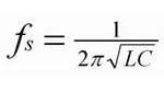
After that, the impedance of the capacitor will appear inductive. It can be seen that the capacitor only has a decoupling effect when the frequency is close to or lower than its SRF, and the capacitor exhibits low resistance at these frequencies.
Typical S11 parameters under different capacitance values are given. From these curves, SRF can be clearly seen. It can also be seen that the larger the capacitance, the better the decoupling performance provided at lower frequencies (the lower the impedance presented).
It is best to place a large-capacity capacitor, such as 2.2μF, at the main node of the Vcc star topology. This capacitor has a low SRF, which is very effective for eliminating low-frequency noise and establishing a stable DC voltage.
Each power pin of the IC requires a low-capacity capacitor (such as 10nF) to filter out high-frequency noise that may be coupled to the power line. For those power supply pins that supply power to noise-sensitive circuits, two external bypass capacitors may be required.
For example: using a 10pF capacitor in parallel with a 10nF capacitor to provide a bypass can provide a wider frequency range of decoupling and try to eliminate the influence of noise on the power supply voltage.
Each power supply pin needs to be carefully inspected to determine how many decoupling capacitors are needed and at which frequency points the actual circuit is susceptible to noise interference.
The combination of good power supply decoupling technology with rigorous PCB layout and Vcc leads (star topology) can lay a solid foundation for any RF system design.
Although there are other factors that reduce the system performance indicators in the actual design, having a noise-free power supply is the basic element for optimizing system performance.
EMC specification for RF PCB design
Layer Distribution
Double-sided board, the top layer is the signal layer, and the bottom surface is the ground plane.
Four-layer board, the top layer is the signal layer, the second layer is the ground plane, and the third layer is the power and control lines.
In special cases (such as the RF signal line passing through the shielding wall), some RF signal lines should be routed on the third layer. Each layer requires a large area of ground.
Grounding
Large-area grounding
In order to reduce the impedance of the ground plane and achieve a good grounding effect, it is recommended to comply with the following requirements:
a) The grounding of RF PCB requires large area grounding;
b) In the microstrip printed circuit, the bottom surface is the ground surface, which must be smooth and flat;
c) The contact surface of the ground should be plated with gold or silver with good electrical conductivity to reduce the resistance of the ground wire;
d) Use fastening screws to make it tightly combined with the shielding cavity, and the spacing of fastening screws is less than λ/20 (depending on the specific situation).
Grounding in close proximity to the group
According to the structure of the circuit and the size of the current, the entire circuit is divided into relatively independent groups. Each group of circuits forms a loop near the ground. The direction of the high-frequency filter capacitors in each group should be adjusted to reduce the power supply loop.
Note that the grounding wire should be short and straight, and it is forbidden to overlap to reduce the interference caused by the common ground impedance.
Grounding of RF devices
When surface-mounted RF devices and filter capacitors need to be grounded, in order to reduce the device grounding inductance, the requirements are as follows.
a) At least 2 wires must be grounded with copper foil;
b) Use at least 2 metallized vias to ground as close as possible to the device pins.
c) Increase the aperture of the via and connect several vias in parallel.
d) The bottom of some components is a grounded metal shell. Grounding holes should be added in the projection area of the component, and no wiring on the surface layer.
Grounding of microstrip circuits
The diameter of the single ground hole of the terminal of the microstrip printed circuit must be larger than the width of the microstrip line, or the terminal must be grounded with a large number of small holes in a row.
Grounding process requirements
a) If the process permits, the distance between the pad and the via can be shortened;
b) If the process permits, the large ground pad can be directly covered on at least 6 ground vias (the specific number varies with the size of the pad);
c) When the ground wire needs to travel a certain distance, the wire length should be shortened, and it is forbidden to exceed λ/20 to prevent the antenna effect from causing signal radiation;
d) Except for special purposes, there must be no isolated copper foil, and ground wire vias must be added to the copper foil;
e) It is forbidden to extend the wire end of the open terminal on the copper foil of the ground wire.
Shielding
Radiofrequency signals can be radiated in the air medium. The greater the spatial distance, the lower the operating frequency, the smaller the parasitic coupling between the input and output terminals, and the greater the isolation. The typical spatial isolation of PCB is about 50dB.
Sensitive circuits and strong radiation source circuits need to be shielded, but if there are difficulties in design and processing (such as space or cost constraints, etc.), they can not be added, but the final decision is to be tested.
These circuits are:
a) The front end of the receiving circuit is a sensitive circuit, and the signal is very small, so shielding should be used.
b) The radio frequency unit and the intermediate frequency unit must be shielded
The intermediate frequency signal of the receiving channel will cause greater interference with the radio frequency signal. On the contrary, the radio frequency signal of the transmitting channel will also cause radiation interference to the intermediate frequency signal.
c) Oscillation circuit
For strong radiation sources, the local oscillator source must be shielded separately. Due to the high level of the local oscillator, it will cause greater radiation interference to other units.
d) Power amplifier and antenna feed circuit
The strong radiation source, and strong signal, must be shielded.
e) Digital signal processing circuit
Strong radiation sources, and the steep upper and lower edges of high-speed digital signals can interfere with analog RF signals.
f) Cascade amplifier circuit
The total gain may exceed the spatial isolation from the output to the input, one of the oscillation conditions is satisfied, and the circuit may self-excited.
If the same frequency gain of the circuit in the cavity exceeds 30-50dB, it is necessary to weld or install a metal shielding plate on the PCB to increase the isolation. In the actual design, the frequency, power, and gain should be considered comprehensively to determine whether to add a shielding plate.
g) Cascaded filtering, switching, and attenuation circuits
In the same shielded cavity, the out-of-band attenuation of the cascade filter circuit, the isolation of the cascade switch circuit, and the attenuation of the cascade attenuation circuit must be less than 30-50 dB.
If this value is exceeded, a metal shielding plate must be soldered or installed on the PCB to increase the isolation.
In the actual design, the frequency, power, and gain should be considered comprehensively to determine whether to add a shielding plate.
h) When the transceiver unit is mixed, it should be shielded.
i) When digital and analog are mixed, the clock line should be covered with copper to isolate or shield the clock line.
Shielding materials and methods
Commonly used shielding materials are all high-conductivity materials, such as copperplate, copper foil, aluminum plate, and aluminum foil. Steel plate, metal plating, conductive coating, etc.
Electrostatic shielding is mainly used to prevent the influence of electrostatic field and constant magnetic field. Should pay attention to two basic points, perfect shielding, and good grounding.
Electromagnetic shielding is mainly used to prevent the influence of alternating magnetic fields or alternating electromagnetic fields. The shielding body is required to have good conductive continuity. The shielding body must be connected to the circuit on the common ground reference plane. The shielding ground in the PCB and the shielded circuit ground is required. Try to get as close as possible.
For some sensitive circuits, circuits with strong radiation sources can be designed with a shielded cavity soldered on the PCB. The PCB must be designed with a via-hole shielding wall, that is, grounding is added to the part of the PCB that is close to the shielding cavity wall. Of vias.
Requirements are as follows.
a) There are more than two rows of vias;
b) The two rows of vias are staggered;
c) The pitch of vias in the same row should be less than λ/20;
d) No solder mask is allowed at the place where the grounded PCB copper foil is crimped with the shielding cavity wall.
RF signal line in the top layer through the shielding wall, the corresponding location in the shielding cavity to open a slot door, door height greater than 0.5mm, and door width to ensure that the installation of the shielding wall between the signal line and the shielding body distance greater than 1mm.
Shield design
The basic structure of the metal shielding cavity
This type of shield is widely used. material is generally thin aluminum alloy, the manufacturing process is generally used punching bending or pressure casting process, this shield has more screw holes, easy to screw fixing. Part of the aluminum cover and absorbing material to enhance the shielding performance.
RF PCB needs to be installed in the shielding cavity, to choose the appropriate size of the shielding cavity, so that its minimum resonant frequency is much higher than the operating frequency, preferably more than 10 times.
The height of the shielding cavity is generally 15-20 times the thickness of the first layer of media or more, in a certain area of the shielding cavity, to increase the minimum resonant frequency of the shielding cavity, it is necessary to increase the aspect ratio, avoid square cavity.
Metal shielding cavity on the PCB layout process requirements
When designing the shield body in contact with the PCB board, the height of the device on the bottom surface of the PCB should be considered, especially the height of the pins of the plug-in device.
It is necessary to consider the size of the screw forbidden area to prevent damage to the surface circuits or devices during assembly. Due to the limitation of the structure size of the RF power amplifier board, the size of the single board is relatively small, so the screw installation space (forbidden wiring area) is generally required to be at least outside the mounting hole pad.
The metal shielding cover itself is very expensive and the assembly cost is very expensive, and it is difficult to ensure high precision and high flatness when manufacturing the metal shielding cover with an irregular shape, and it also restricts the layout of the components; the metal shielding cover is not conducive to the replacement and replacement of components. Fault location.
It is very important to ensure the integrity of the shielding case as much as possible. The digital signal line entering the metal shielding case should go to the inner layer as much as possible. The RF signal line can go out from the small gap at the bottom of the metal shielding case and the wiring layer at the ground gap. Place as much ground as possible around it, and grounds on different layers can be connected together through multiple vias.
In order to ensure assembly and rework, there should be no more than the height of the device within 5mm of the metal shield. The distance between the small chip and the shield should be more than 2mm, the distance between other devices should be more than 3mm, and the orientation should be in accordance with the convenient maintenance direction.
There can be no devices exceeding their height inside the metal shield, and the distance from the top of the device to the surface of the shield must meet the requirements of safety regulations.
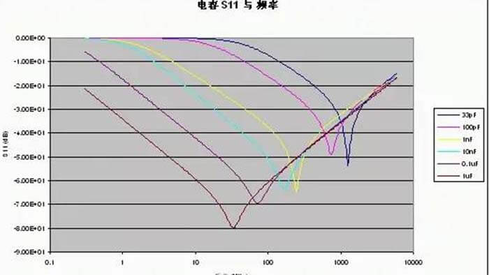
The height matching between the SMA female connector and the PCB board should be considered, otherwise, the soldering reliability will be affected.
As shown in the figure, the PCB thickness tolerance (±10%) and the machining error of the metal shield cavity (±0.05mm) must be considered when designing. It is recommended that the height gap between the SMA microstrip socket and the PCB board should not exceed 0.5mm, and no significant deviation between the socket and the pad is allowed.
Due to the special circumstances of the amplifier board design, allow the signal between the 2 single-board through the shield, and connected with flying wires, as shown in Figure.
RF alignment and ground
We will conduct an RF line simulation of multilayer circuit boards, in order to better make a comparison, the simulation of the PCB is divided into the surface layer before the ground and the ground after the two boards were simulated and compared; the surface layer is not paved PCB file shown in Figure 1 below (two-line widths).
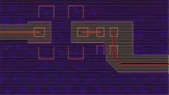
Figure 1a: Line width 0.1016 mm RF line (before the surface lay down)
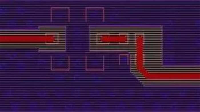
Figure 1b: RF line with a line width of 0.35 mm (before the surface layer is laid)
Figure 1: PCB with surface layer not laid on the ground
First, the two boards with different line widths (before the surface layer is grounded) are imported into SIWAVE by ALLEGRO, and 50 Ω ports are added to the target line. For different line widths of 0.1016mm and 0.35mm, our simulation results are shown in Figure 2, where the curve shown is S21, and the simulation frequency range is 800MHz-1GHz.
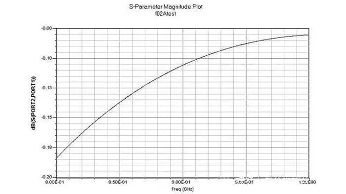
Figure 2a: S21 with unpaved surface layer (line width 0.1016mm)
Figure 2b: S21 with the unpaved surface (line width 0.35mm)
Figure 2: Surface unpaved S21
As can be seen from the figure, in the range of 800 MHz to 1 GHz, the simulated data are displayed in one or two decimal places, and the 0.35 mm loss is one order of magnitude smaller than that of the 0.1016 mm line.
This is due to the characteristic impedance of the 0.35 mm line width being close to 50 Ω under the lamination conditions of the board. Therefore, it is indirectly verified that the impedance calculation we did (using the line width constraint) is somewhat useful.
Next, we did the same simulation after surface layup (800MHz-1GHz), and the imported PCB file is shown below.
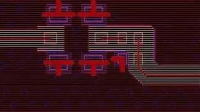
Figure 3a: 0.1016 mm RF line (surface laying)
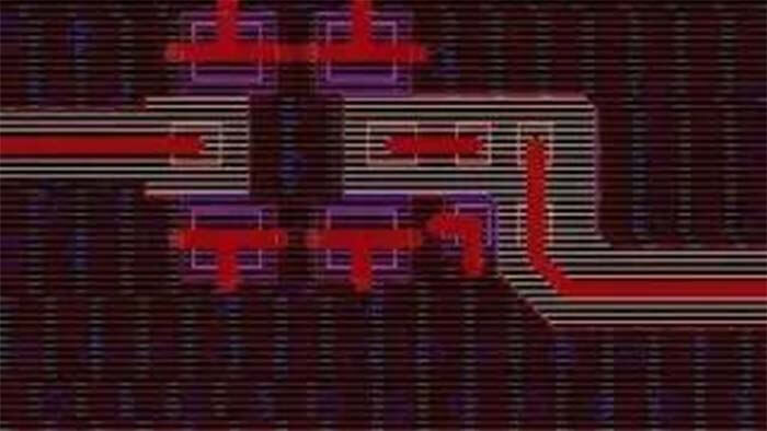
Figure 3b: 0.35 mm RF line (surface layover)
Figure 3: PCB after the surface layer is laid on the ground
The simulation results are shown below:
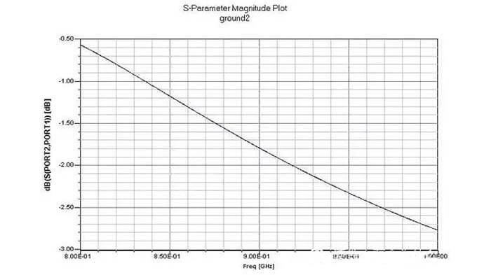
Figure 4a: S21 after surface-layered ground (0.1016 mm)
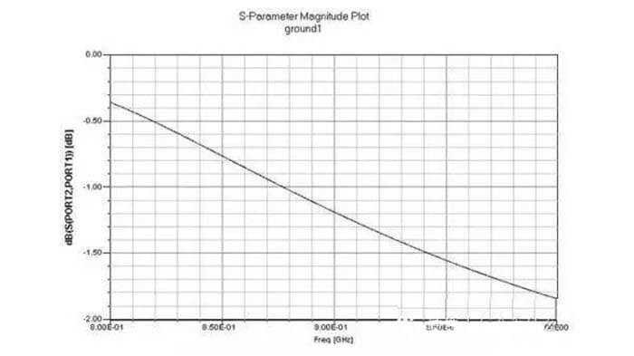
Figure 4b: S21 (0.35mm) after surface laydown
Figure 4: S21 after the surface layer has been laid on the ground
As seen in the figure, the simulated data show that the line loss of the transmission line is already of the order of 1-2 dB, and of course, the 0.35 mm loss is significantly less than that of 0.1016 mm. Another obvious phenomenon is that the loss tends to be larger as the frequency increases from 800 MHz to 1 GHz, relative to the simulation results of the unpaved ground.
We can get such a result from the simulation results – a result: 1. RF alignment is best to go by 50 ohms, which can reduce the line loss;
The peal surface of the pavement is in fact part of the RF signal energy coupled to the ground, resulting in a certain loss. Therefore, the PCB table pavement should be careful. Try to stay away from RF lines. Engineering experience is greater than 1.5 times the line width.
After the reading, have you got the Secrets of RF Circuit Design? or do you want to know more about the Secrets of RF Circuit Design? Welcome to contact our C&T RF engineering team.
These are the Secrets of RF Circuit Design guide, have you got them?
You may also be interested in the below articles.
Internal Antenna VS. External Antenna
LTE Vs. 5G: Is 5G Better Than LTE?