As a PCB engineer, you must master how to quickly design an excellent PCB circuit board, which means that you are on the road to achieving a fast, reliable, and professional-quality PCB.
This article will discuss some concise and key skills and strategies for both novices and experienced printed circuit board (PCB) design.
As long as you pay more attention to these skills in the design process, you and your team can reduce the number of redesigns and shorten the time. Design time and reduce the task of diagnosing the overall design results.
How can we design a successful and excellent PCB circuit board?
1. Familiar with the factory manufacturing process
Many engineers actually don’t know the PCB production steps and chemical treatment processes based on their design files; this is not surprising. However, this lack of practical knowledge often leads novice engineers to make unnecessary and more complex design decisions.
Does the design really need to be so complicated? Can’t it be done with a larger grid to reduce the cost of the circuit board and improve reliability? Other mistakes that novice designers are likely to make, as well as unnecessary under-sized vias and blinds Blind via and buried via.
Those advanced through-hole structures are a weapon for PCB designers, but their effectiveness is highly contextualized. Although they are usable tools, they do not mean that they must be used.
A blog post by PCB design expert Bert Simonovich talked about the issue of through-hole size ratio, through holes with an aspect ratio of 6:1 can ensure that your circuit board can be produced anywhere.
For most designs In other words, with a little thought and planning, you can avoid that high-density (HDI) features and again save costs and improve the manufacturability of the design.
Those ultra-small sizes or single-ended (dead-ended) through-hole copper plating require physical and fluid dynamics capabilities, which not all PCB foundries are good at. Remember, as long as there is a bad via can destroy the entire circuit board; if your design has 20,000 vias, then you have 20,000 chances of failure. Unnecessarily using HDI vias, the failure rate immediately soared.
2. Use an automatic router but don't rely on it
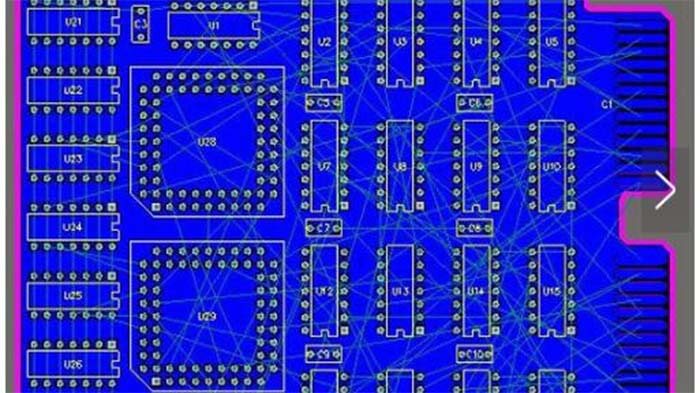
Most professional PCB CAD tools have automatic routers, but unless you design the PCB very professionally, the automatic routers can only be used to make the design preliminary; for the PCB circuit connection, the automatic router is not a one-click For the finished solution, you should still know how to wire it manually.
Auto-router is a highly configurable tool. In order to give full play to their role, router parameters must be carefully and thoughtfully set for each task, and even each module on a single PCB must be individually considered. , In short, there is no proper basic universal preset value.
The process of wiring is more like art like an algorithm. It is a heuristic in itself, so it is very similar to the traditional backtracking algorithm.
The backtracking algorithm is very suitable for finding solutions, especially in situations where path choices such as mazes or puzzles are restricted; but in an open and unrestricted occasion, such as a PCB with pre-placed components, the backtracking algorithm cannot be used.
Find the strengths of the optimized solution. Unless the constraints of the automatic router are carefully fine-tuned by the engineer, the finished wiring still needs to be manually checked for weaknesses in the results of the backtracking algorithm.
The size of the trace is another problem. The auto-router cannot be 100% sure about how much current you intend to pass through a trace, so it cannot help you determine how wide the trace to use; the result is produced by most auto-routers. The trace width does not meet the specifications.
When you consider using an auto-router, ask yourself: “After I set the auto-router constraints for the board, and even set the constraints for each trace on the circuit diagram, how much time do I have? Manual wiring?” Veteran design engineers will put most of their energy into the initial part layout. Almost half of the entire design time is devoted to optimizing the component layout from the following three aspects:
Simplified wiring
Try to minimize the crossing of the fly line (rat’s nest, or the mouse line, the mouse trace net), and so on. The proximity of components-the shorter the winding, the better. Signal timing considerations.
Often use mixed methods for wiring
Manually carry out the critical routing, fix their positions, and then use the automatic routing device to process non-critical routing; the automatic routing area in the design helps to manage the runaway state in the routing algorithm. This method is sometimes A good compromise can be made between the controllability of manual wiring and the speed of automatic wiring.
3. The circuit diagram can simplify the design task
Sometimes just designing a simple circuit board, and drawing schematics (schematic) seems to be a waste of time; especially if you already have experience in completing one or two designs. But for people who are designing PCBs for the first time, drawing circuit diagrams can also be a difficult task.
Skip the circuit diagram is a strategy often adopted by novices and design engineers with moderate experience, but please develop your wiring from a complete circuit diagram that can be used as a reference to help ensure that your wiring connections can be completed. ; The following is the reason.
When designing the PCB, if there is a circuit diagram that can be used as a basic template, it can simplify the wiring task. Use the circuit diagram symbols to complete the connection, and at the same time you can overcome the wiring challenge without having to think about those connections; in the end, you will save the design rework because you have caught the wiring connections that were missed in the first revision.
First of all, the circuit diagram is the visual presentation of the PCB circuit, which can convey multiple levels of information; the sub-regions of the circuit are drawn in detail on several pages, and the components corresponding to the functions can be arranged in adjacent positions, regardless of the final physical layout.
Secondly, since the circuit diagram symbol will mark each pin of each component, it is easy to check the unconnected pins;
Regardless of whether the formal rules describing the circuit are followed or not, the circuit diagram helps you quickly make a visual judgment and ensure the integrity of the circuit.
4. PCB circuit board avoids the risk of splitting
Sliver is a manufacturing error that can be best managed through proper circuit board design; in order to understand the sliver problem, we need to review the chemical etching process.
Chemical etching is to decompose unnecessary copper, but if the part to be etched is particularly long, thin, and flakes, those shapes will sometimes be peeled off before being completely decomposed; such lobes will float in the chemical solution. It may fall randomly on another circuit board.
It is also possible that the risk is that the split remains on the original circuit board; if the split is narrow enough, the acid pool may corrode enough copper below to partially peel off the split. As a result, the slivers stuck to the circuit board like flags and floated around. in the end, they inevitably fell on the board and caused other traces to short-circuit.
5. Consider the board size and current
Most people who are engaged in electronic design know that, just like a river walking along a river, flowing electrons may also encounter throat points and bottlenecks; this is directly applied to the design of an automotive fuse.
By controlling the thickness and shape of the trace (U-shaped bending, V-shaped bending, S-shaped, etc.), the fuse can be calibrated to blow at the throat point when the current is overloaded.
The problem is that design engineers occasionally encounter similar electrical throat points in their PCB designs;
For example, where two steep 45 degrees can be used, a 90-degree bend angle is used; when the bend is greater than 90 degrees, a zigzag shape is used. At best, those wires will only slow down the signal propagation speed; at worst, they will blow at the resistance point like a car fuse.
You may also be interested in the below articles.
Internal Antenna VS. External Antenna
LTE Vs. 5G: Is 5G Better Than LTE?