This is a 2.4GHz wifi antenna design guide with a detailed explanation of the 2.4G WiFi antenna‘s requirements for PCB layout and structure.
With the intensification of market competition, hardware devices are developing in the direction of integration. Antennas have evolved from external to built-in and then embedded. Let’s first introduce the types of antennas for this type of application.
Integrated with PCB etching, limited performance, low cost, used for Bluetooth and WIFI module integration;
Materials include ceramics, metal sheets, PCBs, with moderate performance and cost, suitable for mass embedded RF modules;
Using PCB or FPC+Cable combination, excellent performance, moderate cost, widely used in OTT and terminal equipment;
Plastic rod rubber duck antenna, high performance, independence, high cost, applied to terminal equipment, no need to consider EMC and other issues;
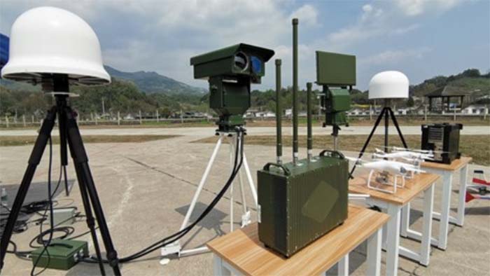
Everyone is familiar with external antennas such as the rubber duck antenna and omnidirectional fiberglass antenna. Let’s take a look directly at the space required by the three types of internal antennas.
Onboard Layout antenna
The onboard Layout antenna is directly formed with the circuit board, which is easy to batch and low cost. The clearance area that needs to be reserved for the antenna is 20*5mm, and it is designed in the corner without metal coverage.
Ceramic patch antenna
The ceramic antenna has the characteristics of small size, easy batch, etc., suitable for BT, WIFI and other conventional demand projects, and it is really connected to the motherboard. The antenna size is 5*2*1mm (length*width*height), and the required space is 11*8mm. The location is best designed in the corner, and there is no metal coverage on the top and bottom of the antenna.
The bracket antenna is usually used in a large space environment and is directly assembled on the client board to form an integrated design of the whole machine. Excellent performance and space-saving. The connection method usually adopts the thimble contact type, and it can also be connected with a cable line.
The PCB antenna FPC antenna connected through the feeder has the characteristics of wide application, free installation, high gain efficiency, and excellent performance. It is installed and fixed by glue or buckle. Usually, it is installed in the casing of the machine.
This type of antenna has a variety of sizes and is suitable for projects with sufficient housing space and high-performance requirements. The actual design requires engineers to match and debug according to the space structure environment.
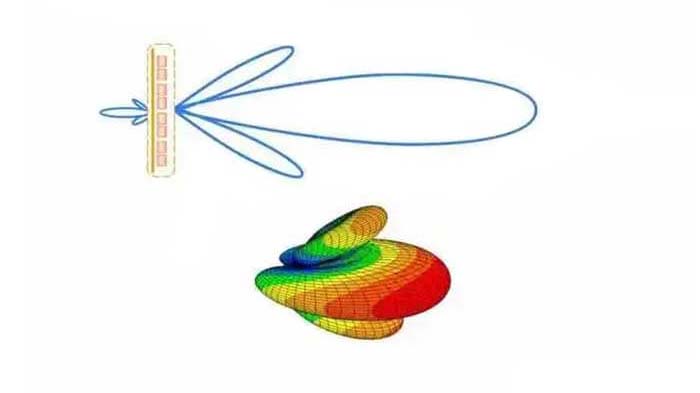
The ultimate goal of the antenna is to radiate radio frequency signals into free space. At this time, the design of the antenna is very important, but the antenna design largely depends on the characteristics of the installed platform. In addition, the antenna is very sensitive to the surrounding environment. In many cases, the antenna is a unique design for each platform.
Since customers are not clear about the factors considered in antenna design, here are some suggestions for portable device antenna design, so that customers can better design their own circuits and PCBs and increase the chances of project success. But each project has its own characteristics, so there are still some problems that require specific analysis.
WiFi antenna design requirements for PCB layout and structure
Antenna form, antenna location, and feed point size recommendations
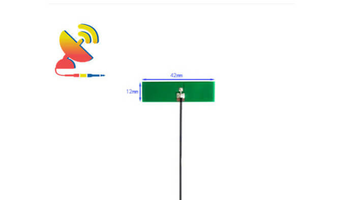
The several forms that the built-in antennas often use are divided into shrapnel forms, chip patch antennas, and FPC antennas. The form of the patch antenna is uniform and has a fixed size. The position and size of the pad are also fixed according to the specific specification of the antenna.
In addition, there are design guidelines for specific antenna types such as clearance requirements around the antenna and recommendations for equipment size.
If using shrapnel form, we recommend that customers use a PIFA antenna as the form of a WiFi antenna. According to our experience, the success rate and performance of the PIFA antenna are better.
The size of the antenna RF feed pad should be 2×3mm, and no copper should be placed on all layers of the PCB with an area of ≥0.8mm surrounding the pad. If it is a PIFA antenna, add a 2×3mm ground pad, and the distance between the two pads is 2mm.
The usual position of the antenna is on the top of the device, starting from the top of the PCB. Cut off the ground of all layers in this area by 2 to 3mm, but keep the pad part of the layer that belongs to the antenna ground pad.
Recommendations for matching circuit wiring
The topological structure of the antenna matching circuit is from the antenna to the test port or Power amplifier. Do not lay the ground under the matching circuit and in the 1.5mm area around the matching network. It is better to place the matching network closer to the feed pad (but not too close).
Microstrip line from WiFi module to antenna matching circuit
The signal transmission line from the WiFi module to the antenna matching circuit is a microstrip line with a characteristic impedance of 50 ohms. In order to avoid loss on the microstrip line, the module should be as close as possible to the antenna. The size of the microstrip line must be determined according to the specific PCB. Crossing lines are not allowed to pass between the microstrip line and the ground.
Some other issues
Grounding
A good RF grounding is undoubtedly very important for the wireless performance of mobile phones. The following design principles must be followed.
Try to make the ground in the outer area as complete as possible and not be damaged by segmentation (the part inside the non-shielding cover). This is especially important for the area near the antenna.
The antenna current must be isolated from the noise current. If the grounding area near the antenna is destroyed to be incomplete, a filled ground plane must be created in the relevant area below it and stitched with ground vias to make it a complete ground.
The wiring in this area must ensure that the antenna current only flows through the surface plane, and the noise current must be restricted from flowing into the complete ground plane inside.
When using a pre-produced antenna, it is important to note that its characteristics depend on the ground plane to which it is connected. Only when the size and shape of the ground plane are consistent with the manufacturer’s evaluation board, can the manufacturer‘s marked specifications be reached?
In other cases, the user needs to measure the impedance of the pre-produced antenna under actual application conditions and match it to the required characteristic impedance.
The use of metal components of the equipment shell
Do not use spraying or plating with metal components on the surface of the housing. The metal plating cannot achieve reliable grounding, which will have a great impact on the performance of the antenna.
Do not use metal decorations near the antenna.
Use of pure metal structural parts
When using all-metal components (such as the front panel or the rear panel), please reserve multiple grounding points for the components used. The specific grounding point location is determined by the antenna design company.
There should be no grounded or ungrounded metal decorations above the antenna radiation area, including electroplating and gold plating.
Consideration of reserving installation location for an antenna
The installation of the antenna should be far away from metal objects, and the antenna needs enough space to expand. If a chip antenna is used, then it is necessary to provide sufficient clearance area and ground of the corresponding size in accordance with the requirements of the application guide.
If a shrapnel antenna is used, support should be designed for the antenna, and the antenna should be fixed on the support, and the support and PCB should be fixed; or without the support, the antenna should be fixed on the shell.
When designing the structure, it is necessary to consider the space and location of the antenna installation, and consider adding a hot-melt column on the bracket or the housing where the antenna is to be installed to fix the antenna.
Consideration of the relative position layout of other modules and antennas
For the relative position of the speaker, camera, vibrator, LCD, battery, other components, and antenna, here are some general suggestions.
The antenna should be far away from the camera and flexible PCB;
The antenna must be at least 5mm away from the battery;
Keep the Vibrator away from the antenna;
The minimum distance between the antenna and the shield is 2-4mm (it will cause parasitic effects);
RF switches and amplifiers or duplexers should be as close as possible to the matching circuit area.
You may also be interested in the below articles.