What is impedance matching? Why do we need impedance matching?
What is impedance?
In a circuit with resistance, inductance, and capacitance, the obstacle to alternating current is called impedance. Impedance is often expressed as Z.
The effective resistance of an electric circuit or component to alternating current arises from the combined effects of ohmic resistance and reactance.
Impedance is composed of resistance, inductive reactance, and capacitive reactance, but it is not a simple addition of the three. If the three are connected in series, and the frequency f, resistance R, inductance L, and capacitance C of the alternating current are known, then the impedance of the series circuit.
The unit of impedance is ohms.
For a specific circuit, the impedance is not constant but changes with frequency. In a series circuit of resistance, inductance, and capacitance, the impedance of the circuit is generally greater than the resistance. That is, the impedance is reduced to a minimum.
In a parallel circuit of inductance and capacitance, the impedance increases to the maximum value at resonance which is the opposite of a series circuit.
What is the impedance matching?
Impedance matching is a part of microwave electronics. In electronics, impedance matching is the practice of designing the input impedance of an electrical load or the output impedance of its corresponding signal source to maximize the power transfer or minimize signal reflection from the load.
It is mainly used on transmission lines to achieve the purpose of all high-frequency microwave signals can be transmitted to the load point, and no signal will be reflected back to the origin, thereby improving energy efficiency.
There are two types of impedance matching, one is to change the impedance (lumped-circuit matching), and the other is to adjust the wavelength of the transmission line (transmission line matching).
To match a group of lines, divide the impedance value of the load point by the characteristic impedance value of the transmission line to normalize, and then plot the value on the Smith chart.
Change resistance
Connect a capacitor or inductance in series with the load to increase or decrease the impedance of the load. The points on the graph will move along the circle representing the real resistance.
If the capacitor or inductance is grounded, the point on the graph will first rotate 180 degrees from the center of the graph, and then move along the resistance circle, and then rotate 180 degrees along the center.
Repeat the above method until the resistance value becomes 1, and then the impedance can be directly changed to zero to complete the matching.
Adjust the transmission line
Lengthen the transmission line from the load point to the source point. The dot on the graph will move counterclockwise along the center of the graph until it reaches the circle with a resistance value of 1. You can add capacitance or inductance to adjust the impedance to zero to complete the matching.
Impedance matching means large transmission power. For a power supply, when its internal resistance is equal to the load, the output power is the largest, and impedance matching is at this time.
The maximum power transmission theorem, if it is high frequency, it means that there is no reflected wave. For ordinary broadband amplifiers, the output impedance is 50Ω, and impedance matching needs to be considered in the power transmission circuit, but if the signal wavelength is much larger than the cable length, that is, the cable length can be ignored, impedance matching is not necessary.
Impedance matching means that during energy transmission, the load impedance is required to be equal to the characteristic impedance of the transmission line. At this time, the transmission will not produce reflection, which indicates that all the energy is absorbed by the load. On the contrary, there is energy loss in transmission.
In order to prevent signal reflection during high-speed PCB wiring, the impedance of the circuit is required to be 50 ohms. This is an approximate figure. Generally, it is stipulated that the baseband of the coaxial cable is 50 ohms, the frequency band is 75 ohms, and the twisted wire is 100 ohms. It is just rounded for the convenience of matching.
Impedance matching refers to a working state in which the load impedance and the internal impedance of the excitation source are adapted to each other to obtain the maximum power output. For circuits with different characteristics, the matching conditions are different.
In a pure resistance circuit, when the load resistance is equal to the internal resistance of the excitation source, the output power is maximum. This working state is called matching, otherwise, it is called a mismatch.
When the internal impedance of the excitation source and the load impedance contains reactance components, in order to obtain the maximum power from the load, the load impedance and the internal resistance must satisfy the conjugate relationship, that is, the resistance components are equal, and the reactance components are only equal in value and opposite in sign.
This matching condition is called conjugate matching.
Impedance matching research
In high-speed design, the impedance matching is related to the quality of the signal.
Series terminal matching
The theoretical starting point of series terminal matching is that under the condition that the signal source end impedance is lower than the characteristic impedance of the transmission line, a resistor R is connected in series between the source end of the signal and the transmission line to match the output impedance of the source end with the characteristic impedance of the transmission line. Suppress the signal reflected from the load end from being reflected again.
The signal transmission after series terminal matching has the following characteristics
- Due to the role of the series matching resistor, when the driving signal is propagated, 50% of its amplitude is propagated to the load end;
- The reflection coefficient of the signal at the load end is close to +1, so the amplitude of the reflected signal is close to 50% of the original signal amplitude.
- The reflected signal is superimposed with the signal propagated at the source end so that the amplitude of the signal received by the load end is approximately the same as the original signal;
- The reflected signal from the load end propagates to the source end, and is absorbed by the matching resistor after reaching the source end;
- After the reflected signal reaches the source end, the source end drives current drops to 0 until the next signal transmission.
Series matching is the most commonly used terminal matching method.
Its advantage is low power consumption, no additional DC load to the driver, no additional impedance between the signal and the ground; and only a resistance element is required.
Parallel terminal matching
The theoretical starting point of parallel terminal matching is that when the impedance of the signal source is very small, the input impedance of the load is matched with the characteristic impedance of the transmission line by increasing the parallel resistance to achieve the purpose of eliminating the reflection at the load. The realization form is divided into two forms single resistance and double resistance.
The signal transmission after parallel terminal matching has the following characteristics
The drive signal propagates along the transmission line approximately at full amplitude;
B All reflections are absorbed by the matching resistor;
C The amplitude of the signal received by the load end is approximately the same as the amplitude of the signal sent by the source end.
In the actual circuit system, the input impedance of the chip is very high, so for the single-resistor form, the parallel resistance value of the load end must be close to or equal to the characteristic impedance of the transmission line.
Assuming that the characteristic impedance of the transmission line is 50Ω, the R-value is 50Ω. If the high level of the signal is 5V, the quiescent current of the signal will reach 100mA. Since the drive capability of a typical TTL or CMOS circuit is very small, this single-resistor parallel matching method rarely appears in these circuits.
Signal transmission
In the multi-layer board signal line of the digital system, the square wave signal is on the multi-layer board transmission line (Transmission Line, which is composed of the signal line, the dielectric layer, and the ground layer) Fast transfers in.
At this time, the transmission line (commonly coaxial cable, Microstrip Line or Strip Line, etc.) can be regarded as a hose, and the pressure applied by the holding tube is like the receiving end of the board (Receiver) The resistor connected in parallel to the Gnd of the component is generally used to adjust the characteristic impedance of its terminal (Characteristic Impedance) to match the internal demand of the receiving end component.
Terminal control technology of transmission line
The signal executes the command correctly in the transmission line to reduce the interference of the messy signal and avoid the wrong action. Once they fail to match each other, there will be a little energy bounce back towards the sending end, which will cause the trouble of reflection noise.
When the characteristic impedance (Z0) of the transmission line itself is set at 28 ohms by the designer, the grounding resistor (Zt) of the terminal control must also be 28 ohms, to assist the transmission line to maintain Z0 and stabilize the whole at 28 ohms, the design value of ohm.
Only in this matching situation of Z0=Zt, the signal transmission will be the most efficient, and its signal integrity (Signal Integrity) will also be the best.
Characteristic Impedance
When a square wave of a signal moves forward with a high-level positive pressure signal in the signal line of the transmission line assembly, it will be in the nearest reference layer (such as the ground layer).
Theoretically, the negative pressure signal induced by the electric field must accompany it forward (equal to the return path of the positive pressure signal), so that the overall loop system can be completed.
If the flight time of the signal is temporarily frozen while it is moving forward, you can imagine the instantaneous impedance presented by the signal line, dielectric layer, and reference layer.
This is the so-called characteristic impedance. The characteristic impedance should be related to the line width (w), line thickness (t), dielectric thickness (h), and dielectric constant (Dk) of the signal line.
Consequences of poor impedance matching
Since the original term of the characteristic impedance (Z0) of the high-frequency signal is very long, it is generally referred to as impedance for short.
This is not exactly the same as the impedance value (Z) that appears in low-frequency AC alternating current (60Hz) and its wires (not transmission lines).
In digital systems, when the Z0 of the entire transmission line can be managed properly, and if it is controlled within a certain range (±10% or ±5%), this high-quality transmission line will reduce noise and prevent misoperations.
However, when any one of the four variables (w, t, h, r) of Z0 in the above microstrip line is abnormal, such as a gap in the signal line, the original Z0 will rise suddenly (see Z0 and Z0 in the above formula). The fact that W is inversely proportional).
When it is unable to continue to maintain its due stability and uniformity (Continuous), the energy of the signal will inevitably advance partly, and partly bounce back and reflect the lack of reflection. Explain the above-mentioned problem of poor characteristic impedance matching.
Poor impedance matching causes noise
The above-mentioned part of the signal energy rebound will cause the original good-quality square wave signal to be abnormally deformed immediately (that is, the overshoot of the high level upward, the undershoot of the low level downward, and the subsequent ringing of the two).
When the high-frequency noise is severe, it will cause malfunction, and the faster the pulse speed, the more noise and the easier it is to make mistakes.
When should impedance matching be considered?
In an ordinary broadband amplifier, because the output impedance is 50Ω, it is necessary to consider impedance matching in the power transmission circuit. However, in fact, when the length of the cable is negligible for the wavelength of the signal, there is no need for impedance matching.
Consider the signal frequency is 1MHz, its wavelength is 300m in the air, and about 200m in the coaxial cable. In the commonly used coaxial cable with a length of about 1m, it is within a completely negligible range.
If there is impedance, power consumption will occur in the impedance, so if impedance matching is not done, the output power of the amplifier will be wasted uselessly.
Analyze characteristic impedance
In recent years, an increasingly important issue in the field of high-speed design is the design of circuit boards with controlled impedance and the characteristic impedance of interconnect lines on the circuit board.
What is a transmission line?
Two conductors with a certain length form a transmission line.
One of the conductors becomes a signal propagation path, and the other conductor constitutes the signal return path (ground).
In a multi-layer circuit board design, each PCB interconnection line constitutes a conductor in the transmission line, and the transmission line uses the adjacent reference plane as the second conductor or signal return path of the transmission line.
What kind of PCB interconnection line is a good transmission line?
Generally, if the characteristic impedance is consistent everywhere on the same PCB interconnection line, such a transmission line becomes a high-quality transmission line.
What kind of circuit board is called a controlled impedance circuit board?
A controlled impedance circuit board means that the characteristic impedance of all transmission lines on the PCB meets a unified target specification. It usually means that the characteristic impedance of all transmission lines is between 25Ω and 70Ω.
A signal point of view
The most effective way to consider the characteristic impedance is to look at what the signal itself sees as it propagates along the transmission line.
To simplify the discussion of the problem, it is assumed that the transmission line is a microstrip type, and the cross-section of the transmission line is consistent when the signal propagates along the transmission line.
Add a step signal with an amplitude of 1V to the transmission line. The step signal is a 1V battery, which is connected by the front end and connected between the signal line and the return path.
At the moment when the battery is switched on, the signal voltage waveform will travel in the dielectric at the speed of light, which is usually about 6 inches/ns.
The signal is defined as the voltage difference between the signal line and the return path, which is always obtained by measuring the voltage difference between any point on the transmission line and the adjacent signal return path.
The signal is forwarded along the transmission line at a speed of 6 inches/ns. In the first 10ps time interval, the signal traveled a distance of 0.06 inches along the transmission line.
Assuming that the lock time is at this moment, consider what happens on the transmission line. Over this distance of travel, the transmission of the signal establishes a stable constant signal with an amplitude of 1V between this section of the transmission line and the corresponding adjacent signal return channel.
This means that extra positive charges and extra negative charges have been accumulated on this section of the transmission line and the corresponding return path to establish this stable voltage.
It is the difference in these charges that establishes and maintains a stable 1 V voltage signal between the two conductors, and the stable voltage signal between the conductors establishes a capacitance between the two conductors.
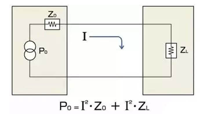
Resistance is a real physical component. Through Ohm’s law, we can know the relationship between voltage, current, and resistance, U=I*R
We analyze the specific relationship between these three through a specific circuit, please see the simplest circuit diagram below. This circuit diagram consists of only a power supply, a resistor, and some wires.
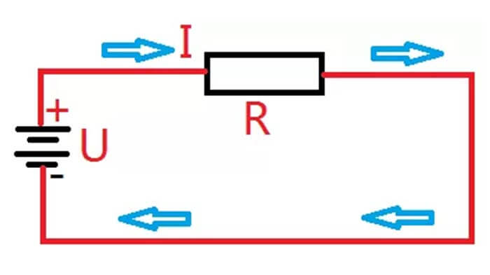
The resistance of this resistor can also be measured directly with a multimeter.
In fact, the characteristic impedance is a physical quantity that is closely separated from the radiofrequency. Before understanding the characteristic impedance, let’s first understand the radio frequency.
We know that radio stations, mobile phone communication signals, wifi, etc. are all devices that transmit signal energy to the outside, that is to say, the energy is emitted from the antenna, and the energy does not return to the antenna.
The radio frequency signal transmitted on the wire that transmits radiofrequency energy is also the same. I hope that it will not be transmitted back to the past. If there is energy back transmitted back, it means that the transmission effect is poor.
We know that resistance = voltage/current. In fact, the characteristic impedance also has this relationship: characteristic impedance = RF voltage/RF current.
For the same RF voltage, the current relationship is i2=twice i1. The wider the line, the smaller the characteristic impedance will be.
The difference between characteristic impedance and resistance, for the same board, the characteristic impedance is related to line width, but not to length.
In fact, there are many factors that affect the characteristic impedance, including the material, the distance between the wire and the bottom plate, and many other factors.
The characteristic impedance of a wire is the size of the resistance of the wire to the radio frequency energy transmitted on it.
Recognize reflections on transmission lines
Above we assumed that the wire is infinitely long, but the actual wire length is finite. When the RF signal reaches the end of the wire, there is no way to release the energy, and it will travel back along the wire.
Resistance is a component that consumes energy.
We found that there are three special cases.
When R=RO, the transmitted energy is just absorbed by the resistance R at the end, and no energy is reflected back. It can be seen that this wire is wireless.
When R=∞ (open circuit), all the energy is reflected back, and the endpoint of the line will produce a voltage twice that of the emission source.
When R=0, the endpoint will reflect back -1 times the source voltage.
Understanding impedance matching
Impedance matching refers to a working state in which the load impedance and the internal impedance of the excitation source are adapted to each other to obtain the maximum power output.
Impedance matching is for radiofrequency and so on, but it is not applicable to power circuits, otherwise, things will be burned.
We often hear that the characteristic impedance is 50 ohms, 75 ohms, etc. Where did these 50 ohms come from? Why is it 50 ohms instead of 51 ohms, or 45 ohms?
This is an agreement, 50 ohms should be said to have a better transmission effect for general radio frequency circuits.
Wires and cables need to be 50 ohms because the circuit load is equivalent to 50 ohms resistance. If you make wires with other impedance values, they will not match the load. The farther the deviation is, the worse the transmission effect will be!
In the process of PCB design, before routing, we generally stack the items we want to design and calculate the impedance based on the thickness, base material, number of layers, and other information. After the calculation, the following figure can generally be obtained.
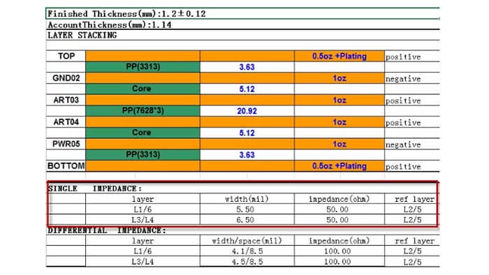
Figure 1 Illustration of overlay information
As can be seen from the above figure, the single-ended network design above is generally controlled by 50 ohms, so many people will ask, why is it required to control according to 50 ohms instead of 25 ohms or 80 ohms?
First of all, 50 ohms are selected by default, and the PCB connected to various cables is also in accordance with the 50-ohm impedance standard for impedance matching.
Secondly, the formulation of general standards will be based on comprehensive consideration of the PCB production process and design performance and feasibility.
From the perspective of PCB production and processing technology, considering the equipment of most existing PCB manufacturers, it is relatively easy to produce PCBs with a 50-ohm impedance.
From the impedance calculation process, it can be seen that a too-low impedance requires a wider line width, and a thin medium or a larger dielectric constant, which is more difficult to satisfy in terms of space for the current high-density boards;
Too high an impedance requires a thinner line width, a thicker medium, or a smaller dielectric constant, which is not conducive to the suppression of EMI and crosstalk. At the same time, for multilayer boards and from the perspective of mass production, the reliability of processing will be affected poorly.
Control 50-ohm impedance. Under the environment of using common boards (FR4, etc.) and common core boards, produce products with common board thicknesses (such as 1mm, 1.2mm, etc.). Common line widths (4~10mil) can be designed. The factory is very convenient to process, and the equipment requirements for its processing are not very high.
From the perspective of PCB design, 50 ohms is also selected after comprehensive consideration. From the performance of PCB traces, the low impedance is generally better. For a transmission line of given line width, the closer the distance to the plane is, the corresponding EMI will be reduced, and the crosstalk will also be reduced.
However, from the perspective of the full signal path, one of the most critical factors needs to be considered, that is, the drive capability of the chip. In the early days, most chips could not drive transmission lines with an impedance less than 50 ohms, and transmission lines with higher impedance were inconvenient to implement. Therefore, a 50-ohm impedance is used as a compromise.
Therefore, 50 ohms is generally selected as the default value of the single-ended signal control impedance in normal time.
You may also be interested in the below articles.